Micron Surpasses Expectations with Advanced HBM4 Memory Technology
Micron Technology has announced its fourth-quarter and full-year fiscal 2025 results, exceeding market expectations and offering significant updates on its next-generation High Bandwidth Memory (HBM) technology. During the earnings call, CEO Sanjay Mehrotra confirmed that Micron’s HBM4 memory will be available next year, featuring several enhancements that go beyond the standard JEDEC HBM4 specification.
HBM4: Setting New Industry Benchmarks
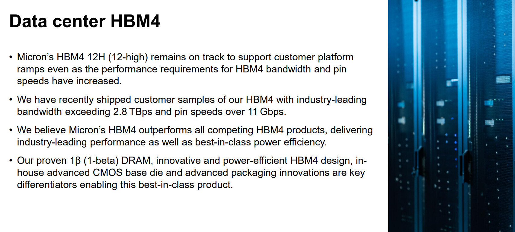
Micron’s HBM4 12-high memory is on schedule to support customer platform rollouts, even as industry demands for bandwidth and pin speeds continue to rise. According to Mehrotra, Micron has already shipped customer samples of its HBM4, which deliver industry-leading bandwidth exceeding 2.8 TB/s and pin speeds over 11 Gbps. For comparison, the JEDEC HBM4 standard specifies 2 TB/s bandwidth and 8 Gbps pin speeds across a 2048-bit interface. Micron’s advancements represent a 40% increase in bandwidth, setting a new performance benchmark for HBM memory.
This leap in performance is driven by the needs of major customers such as NVIDIA, who require increasingly powerful memory solutions to match the rapid growth of their compute architectures. To meet these demands, Micron is pushing beyond JEDEC standards, leveraging its expertise in DRAM technology and advanced packaging.
Innovative Design and Customization for Next-Gen Accelerators
Micron’s HBM4 stands out not only for its performance but also for its power efficiency. The company attributes this to its proven 1-gamma DRAM process, innovative and energy-efficient HBM4 design, in-house advanced CMOS base die, and cutting-edge packaging techniques. These differentiators position Micron’s HBM4 as a leading solution in the high-performance memory market.
Looking ahead, Micron plans to offer both standard and customizable options for its HBM4E products. This includes the ability to customize the base logic die, a feature that is gaining traction among leading accelerator manufacturers like NVIDIA and AMD. For the first time, these companies are set to utilize customized HBM memory stacks, which can include a base die with tailored logic or accelerator circuitry. This approach enables more efficient data routing, reduced latency, and improved overall performance for AI and high-performance computing workloads.
The integration of a custom base die—potentially serving as a data processing or logic layer—marks a significant step forward in memory architecture. By embedding specialized logic within the HBM stack, NVIDIA and AMD aim to achieve performance levels that surpass those of conventional third-party ASIC solutions, further advancing the capabilities of next-generation accelerators.