TSMC’s 2nm N2 Node: Early Adopters and Industry Impact
TrendForce has released insights into the initial customers set to adopt TSMC’s advanced 2nm N2 semiconductor manufacturing process. This next-generation node is poised to drive significant innovation across the tech industry, with several major players already preparing to leverage its capabilities for their upcoming products.
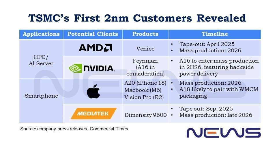
Apple Leads the Charge with 2nm Technology
Apple is expected to be the largest early adopter of TSMC’s 2nm N2 node. The company plans to utilize this cutting-edge process for its forthcoming A20 chip, which will power the next generation of iPhones. Additionally, Apple’s M6 series processors, designed for future Mac computers, and the Vision Pro R2 chip, intended for the next iteration of its AR wearable, are both set to benefit from the enhanced performance and efficiency of the N2 node. Mass production for these chips is anticipated to begin in 2026.
AMD and MediaTek Join the 2nm Wave
AMD and MediaTek are also among the first companies to implement TSMC’s 2nm process. AMD is developing CPU Core Dies (CCDs) for its EPYC “Venice” server processors, which will be based on the upcoming “Zen 6” microarchitecture. The tape-out for the Zen 6 CCD was completed in April 2025, with mass production expected to follow in 2026.
MediaTek, a leading player in the mobile SoC market, is preparing its next flagship chipset, the Dimensity 9600 series, using the N2 node. The Dimensity 9600 recently completed tape-out, and mass production is projected for late 2026.
NVIDIA Eyes Advanced Nodes for Future GPUs
NVIDIA, known for producing some of the largest chips by die area at TSMC, is preparing its next-generation “Feynman” GPU architecture to succeed the upcoming “Rubin” series. While TrendForce indicates that “Feynman” will utilize a 2nm-class node with mass production scheduled for the second half of 2026, reports suggest NVIDIA may opt for TSMC’s even more advanced A16 node, which features backside power delivery. The A16 node is expected to be a 1.6nm or 16 Angstrom-class process, offering further improvements in performance and efficiency.
Intel’s Strategic Shift Away from TSMC’s 2nm Node
Notably absent from the list of early 2nm adopters is Intel. Currently, Intel relies on TSMC’s 3nm N3B node for the compute tiles in both its server and client processors. However, Intel is shifting focus to its own in-house foundry technologies, with plans to utilize the Intel 18A node, which incorporates RibbonFET and PowerVia innovations, for its next-generation processors. Intel has publicly confirmed this transition and is also developing the more advanced Intel 14A node for future products. The company’s strategic direction underscores its commitment to regaining process leadership and reducing reliance on external foundries.
Looking Ahead: The Future of Semiconductor Manufacturing
The adoption of TSMC’s 2nm N2 node by industry leaders such as Apple, AMD, MediaTek, and potentially NVIDIA marks a significant milestone in semiconductor manufacturing. As mass production ramps up in 2026, these advancements are expected to deliver substantial gains in performance, power efficiency, and device capabilities, shaping the next era of computing and consumer electronics.