Rapidus to Deliver 2 nm Process with High Transistor Density
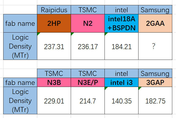
According to Korean analyst Kurnal on X, Rapidus, the Japanese foundry pushing into leading-edge chips, is set to release its upcoming 2 nm process, known as 2HP. This new process boasts a transistor density that competes with the best in the industry, including TSMC. The reported logic density for 2HP is 237.31 million transistors per square millimeter, which is on par with TSMC's N2 at 236.17 MTr/mm², and surpasses Intel's 18A at 184.21 MTr/mm². Rapidus has focused on high-density standard cells and a single-wafer front-end method that allows for tuning runs before scaling. A gate-all-around test chip built with ASML EUV tools has successfully met its electrical targets. The company plans to release process design kits in early 2026 and aims to begin high-volume production at its IIM-1 facility in 2027, with an expected monthly output of around 25,000 wafers.
What sets Rapidus apart from its competitors is its emphasis on speed and flexibility. While slightly behind TSMC in terms of node advancement in 2027, Rapidus promises significantly shorter cycle times compared to traditional batch processes. This reduction in turnaround time from 120 days to approximately 50 days, with the ability to expedite "hot lot" orders in as little as 15 days for urgent requests. To achieve this, Rapidus is developing a custom backend ecosystem with OSATs, EDA vendors, IP providers, and materials partners. The company also benefits from government support and interest from major players in the computing industry. However, while transistor density is important, other factors such as energy efficiency, performance per watt, supply chain maturity, and consistent yields will ultimately determine Rapidus' success in becoming a reliable, high-volume competitor in the market.