GeForce RTX 5090 "Blackwell" Leak
Check out the latest image of what is believed to be the upcoming GeForce RTX 5090 "Blackwell," the successor to the RTX 4090 "Ada." The leaked picture showcases the massive GPU and layout that align with previous bare PCB leaks over the weekend.
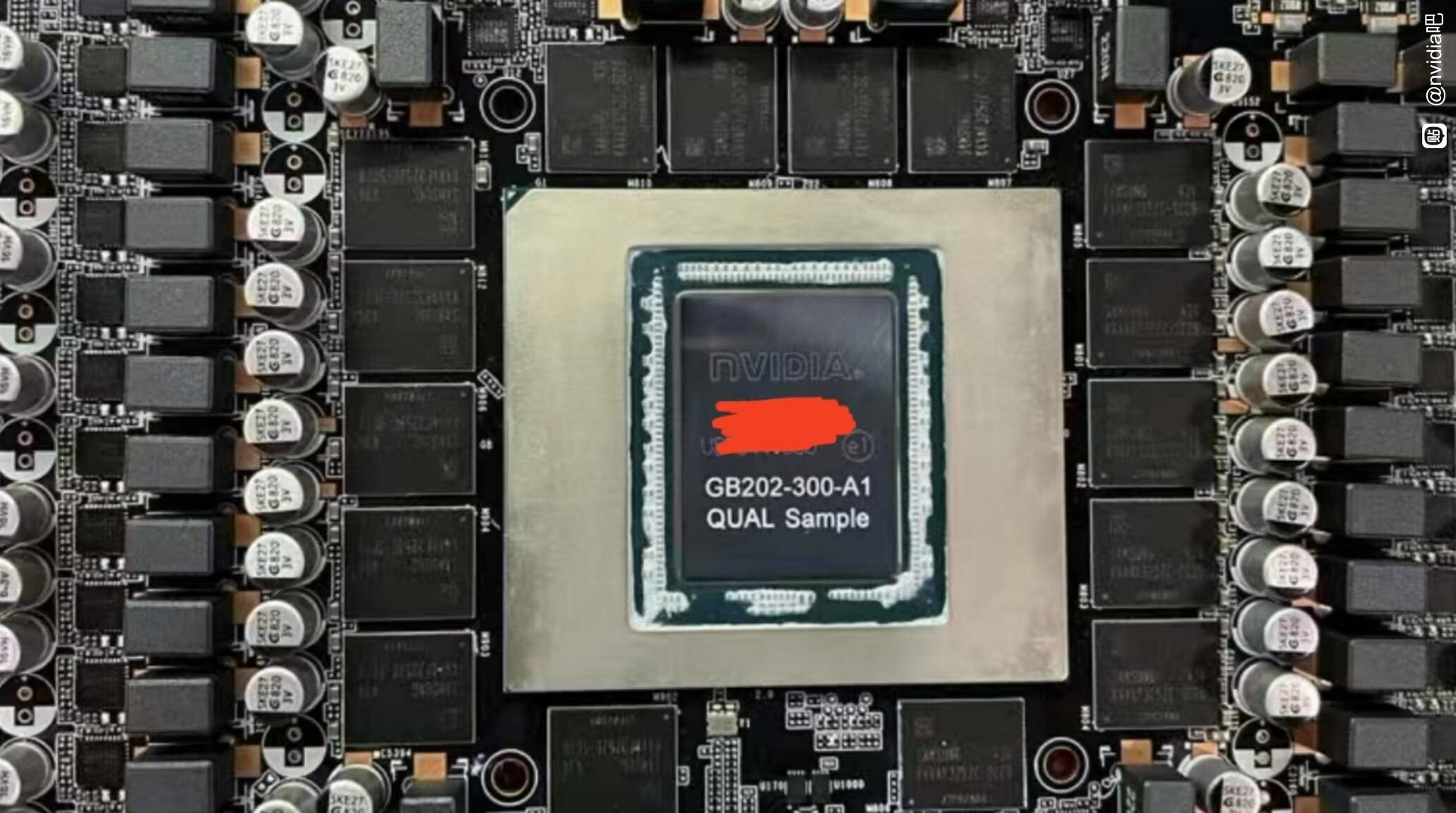
The RTX 5090 is powered by the "GB202" silicon, which is the largest gaming GPU based on the "Blackwell" graphics architecture. The silicon in the image bears the ASIC code "GB202-300-A1," indicating that the RTX 5090 may not utilize all available SM units, as fully utilized NVIDIA ASICs typically have the variant designation "450."
Surrounding the "GB202" ASIC are sixteen GDDR7 memory chips, totaling 32 GB of memory for the RTX 5090. The chip count, along with the large GPU package size and high pin-count, suggest that the "GB202" features a 512-bit wide memory bus. With an assumed memory speed of 28 Gbps, this memory bus is expected to deliver an impressive memory bandwidth of 1,792 GB/s.
The GPU and memory components are supported by the card's 24-phase VRM solution, drawing power from a single 16-pin 12V-2x6 power connector. NVIDIA is likely to push the limits of the 600 W continuous power-delivery capability of the connector, giving the card a total graphics power (TGP) of around 500-550 W, if not more.